- 您现在的位置:买卖IC网 > Sheet目录3872 > PIC16C57C-04/P (Microchip Technology)IC MCU OTP 2KX12 28DIP
PIC18F2450/4450
2006 Microchip Technology Inc.
Advance Information
DS39760A-page 81
EXAMPLE 6-3:
WRITING TO FLASH PROGRAM MEMORY (CONTINUED)
6.5.2
WRITE VERIFY
Depending on the application, good programming
practice may dictate that the value written to the
memory should be verified against the original value.
This should be used in applications where excessive
writes can stress bits near the specification limit.
6.5.3
UNEXPECTED TERMINATION OF
WRITE OPERATION
If a write is terminated by an unplanned event, such as
loss of power or an unexpected Reset, the memory
location just programmed should be verified and
reprogrammed if needed. If the write operation is
interrupted by a MCLR Reset or a WDT Time-out Reset
during normal operation, the user can check the
WRERR bit and rewrite the location(s) as needed.
6.5.4
PROTECTION AGAINST SPURIOUS
WRITES
To protect against spurious writes to Flash program
memory, the write initiate sequence must also be
followed. See Section 18.0 “Special Features of the
CPU” for more detail.
6.6
Flash Program Operation During
Code Protection
Protection” for details on code protection of Flash
program memory.
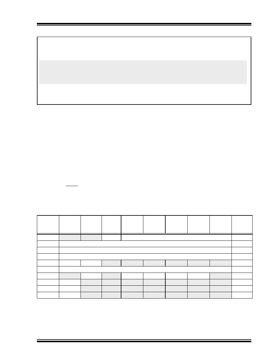
TABLE 6-2:
REGISTERS ASSOCIATED WITH PROGRAM FLASH MEMORY
PROGRAM_MEMORY
BCF
EECON1, CFGS
; access Flash program memory
BSF
EECON1, WREN
; enable write to memory
BCF
INTCON, GIE
; disable interrupts
MOVLW
55h
Required
MOVWF
EECON2
; write 55h
Sequence
MOVLW
0AAh
MOVWF
EECON2
; write 0AAh
BSF
EECON1, WR
; start program (CPU stall)
DECFSZ
COUNTER1
BRA
WRITE_BUFFER_BACK
BSF
INTCON, GIE
; re-enable interrupts
BCF
EECON1, WREN
; disable write to memory
Name
Bit 7
Bit 6
Bit 5
Bit 4
Bit 3
Bit 2
Bit 1
Bit 0
Reset
Values
on page
TBLPTRU
—
bit 21
Program Memory Table Pointer Upper Byte (TBLPTR<20:16>)
TBPLTRH
Program Memory Table Pointer High Byte (TBLPTR<15:8>)
TBLPTRL
Program Memory Table Pointer Low Byte (TBLPTR<7:0>)
TABLAT
Program Memory Table Latch
INTCON
GIE/GIEH PEIE/GIEL TMR0IE
INT0IE
RBIE
TMR0IF
INT0IF
RBIF
EECON2
Control Register 2 (not a physical register)
EECON1
—CFGS
—
FREE
WRERR
WREN
WR
IPR2
OSCFIP
—
USBIP
—
HLVDIP
—
PIR2
OSCFIF
—
USBIF
—
HLVDIF
—
PIE2
OSCFIE
—
USBIE
—
HLVDIE
—
Legend: — = unimplemented, read as ‘0’. Shaded cells are not used during Flash access.
发布紧急采购,3分钟左右您将得到回复。
相关PDF资料
PIC16CE623-04/SO
IC MCU OTP 512X14 EE COMP 18SOIC
PIC16C57C-04/SP
IC MCU OTP 2KX12 28DIP
PIC16LF628A-I/SO
IC MCU FLASH 2KX14 EEPROM 18SOIC
PIC16C55A-20/SO
IC MCU OTP 512X12 28SOIC
PIC24F16KA101-I/MQ
IC PIC MCU FLASH 16KB 20-QFN
PIC16F627-04/SO
IC MCU FLASH 1KX14 COMP 18SOIC
PIC16C58B-20I/P
IC MCU OTP 2KX12 18DIP
PIC24FJ16GA002-I/SS
IC PIC MCU FLASH 16K 28-SSOP
相关代理商/技术参数
PIC16C57C-04/P
制造商:Microchip Technology Inc 功能描述:IC 8BIT CMOS MCU 16C57 DIP28
PIC16C57C-04/P
制造商:Microchip Technology Inc 功能描述:28 Pin 3 KB OTP 72 RAM 20 I/O
PIC16C57C-04/P072
制造商:Microchip Technology Inc 功能描述:
PIC16C57C-04/P073
制造商:Microchip Technology Inc 功能描述:
PIC16C57C-04/SO
功能描述:8位微控制器 -MCU 3KB 72 RAM 20 I/O RoHS:否 制造商:Silicon Labs 核心:8051 处理器系列:C8051F39x 数据总线宽度:8 bit 最大时钟频率:50 MHz 程序存储器大小:16 KB 数据 RAM 大小:1 KB 片上 ADC:Yes 工作电源电压:1.8 V to 3.6 V 工作温度范围:- 40 C to + 105 C 封装 / 箱体:QFN-20 安装风格:SMD/SMT
PIC16C57C-04/SO
制造商:Microchip Technology Inc 功能描述:8BIT CMOS MCU SMD 16C57 SOIC28
PIC16C57C-04/SP
功能描述:8位微控制器 -MCU 3KB 72 RAM 20 I/O RoHS:否 制造商:Silicon Labs 核心:8051 处理器系列:C8051F39x 数据总线宽度:8 bit 最大时钟频率:50 MHz 程序存储器大小:16 KB 数据 RAM 大小:1 KB 片上 ADC:Yes 工作电源电压:1.8 V to 3.6 V 工作温度范围:- 40 C to + 105 C 封装 / 箱体:QFN-20 安装风格:SMD/SMT
PIC16C57C-04/SP
制造商:Microchip Technology Inc 功能描述:IC 8BIT CMOS MCU 16C57 SDIL28